In a previous article, I have shown you how you can build your own switched capacitor voltage converter circuit using the classic industry-standard LMC7660 IC. But oftentimes there are situations when you don’t have a specific IC available or the cost of an additional IC is ruining the harmony of your BOM. And this is where our beloved 555 timer IC comes to rescue. That is why to reduce the pain of finding a specific chip for a specific application and also to reduce the BOM cost; we are going to use our beloved 555 timers to build, demonstrate and test a positive and a negative charge pump circuit with a 555 timer IC.
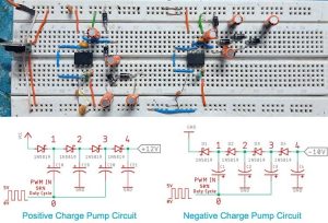
What is a Charge Pump Circuit?
A charge pump is a type of circuit that is made out of diodes and capacitors by configuring the diodes and capacitors in a specific configuration to get the output voltage higher than the input voltage or lower than the input voltage. By lower, I mean to say negative voltage with respect to ground. Also, alike every circuit, this circuit has some advantages and disadvantages which we will discuss later in the article.
To know how the circuit works, we need to look into the schematic of both, the charge pump booster and charge pump inverter circuit first.
Charge Pump Booster Circuit
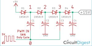
To understand the circuit better, let’s assume we are using ideal diodes and capacitors to build the circuit shown in Figure-1. Also, we are assuming that the circuit reached a steady-state and the capacitors are fully charged up. Furthermore, we have no load connected to this circuit with these conditions in mind the working principle is described below.
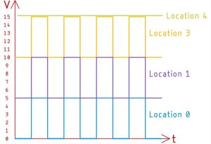
With the help of Figure 1 and Figure 2, We are going to explain how a charge pump circuit works.
Now let’s assume that we have connected a PWM signal from a signal generator and the signal oscillates within 0-5V.
When the input PWM signal at location-0 is in 0V state, the Voltage at location-1 is +5V or VCC. So, that’s why the capacitor got charged up to +5V or VCC. And in the next cycle, when the PWM signal switches from 0V to 5V, the voltage at location 1 is now +10V. If you observe Figure 1. & Figure 2. You can observe why the voltage got doubled.
It doubled because the reference at the capacitor’s terminal got sifted and as the current cannot flow in the reverse direction through the diode because of diode action so, at location 1 we end up with a shifted square wave which is above the bias voltage or input voltage. Now, you can understand the effect in Figure 2, location 1 of the waveform.
After that, the signal is fed to a classic single diode rectifier circuit to smooth out the square wave and get +10V DC voltage at the output.
In the next stage at Location 2, the voltage is +10V, you can verify that from Figure 1. Now in the next cycle, the same phenomenon happens again we end up with +15V output at location 4 after the final rectification is done with the diode and capacitors.
This is how the charge pump boost circuit works.
Next, we will see how a charge pump inverter or a negative charge pump works.
Charge Pump Inverter
The negative voltage charge pump is a little tricky to explain, but please stay with me and I will explain how it works.
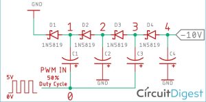
In the first cycle at location-0 of Figure-3, the input signal is 0V and nothing is happening but as soon as the PWM signal reaches 5V at location-0, the capacitors start to charge up through the diode D1 and soon it will have 5V at location-1. And now we have a diode that is in a forward-bias condition so the voltage will become 0V at location-1 almost instantly. Now when the input PWM signal goes low again the voltage at location-1 is 0V. At this moment the PWM signal will subtract the value and we will get -5V at location 1.
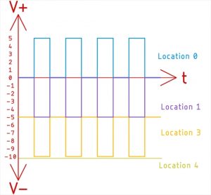
And now the classic single diode rectifier will do its job and convert the pulsed signal into a smooth DC signal and store the voltage at capacitor C2.
In the next stage of the circuit which is location-3 and location-4, the same phenomenon will happen simultaneously and we will get a steady -10V DC at the output of the circuit.
And this is how the circuit for a negative charge pump actually works.
Note! Please note that I did not mention location 2 at this point because as you can see from the circuit at location 2 the voltage would be -5V.
Components Required
- NE555 Timer IC – 2
- LM7805 Voltage Regulator IC – 1
- 0.1 uF Capacitor – 4
- 0.01uF Capacitor – 2
- 4.7uF Capacitor – 8
- 1N5819 Schottky Diode – 8
- 680 Ohm Resistor – 2
- 330 Ohm Resistor – 2
- 12V DC Power Supply – 1
- Generic Single Guage Wire – 18
- Generic Breadboard – 1
Schematic Diagram
Circuit for the Charge Pump Booster:
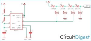
For demonstration, the circuit is constructed on a solderless breadboard with the help of the schematic. All the components are placed as close and as tidier as possible to decrease unwanted noise and ripple.
Calculations
The PWM frequency and the duty cycle of the 555 timer IC need to be calculated so, I have gone ahead and calculated the frequency and duty cycle of the 555 timers with the help of this 555 Timer Astable Circuit Calculator tool.
For the practical circuit, I have used a fairly high frequency of 10 kHz in order to reduce the ripple in the circuit. Shown below is the calculation
Source: Positive and Negative Charge Pump Circuit
The post Positive and Negative Charge Pump Circuit appeared first on PIC Microcontroller.
from Blog – PIC Microcontroller https://ift.tt/3itReXu


No comments:
Post a Comment
Please do not enter any spam link in the comment box.